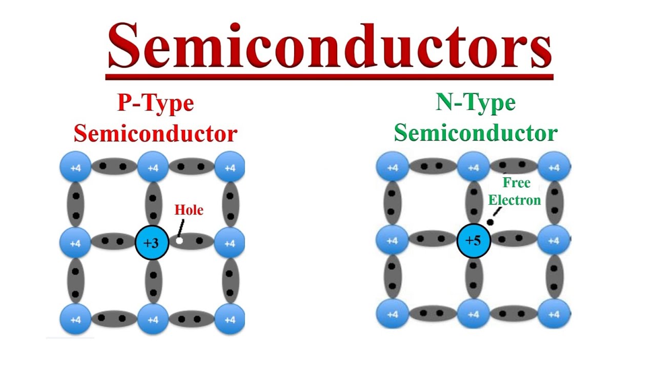

Semiconductors are materials whose electrical conductivity falls between that of conductors and insulators. By adding small amounts of specific impurities, their electrical properties can be controlled. This process is known as doping.
Based on the type of impurity added, semiconductors are mainly classified as P-type and N-type semiconductors.
What Is a P-Type Semiconductor?
A P-type semiconductor is formed by doping an intrinsic semiconductor, such as silicon or germanium, with a trivalent impurity.
Trivalent impurities have three valence electrons.
Common examples include:
- Boron
- Aluminium
- Gallium
- Indium
When a trivalent atom replaces a silicon atom in the crystal lattice, one covalent bond lacks an electron. This creates a hole, which can act as a positive charge carrier.
Therefore, holes are the majority charge carriers in a P-type semiconductor, while electrons are the minority carriers.
What Is an N-Type Semiconductor?
An N-type semiconductor is formed by doping an intrinsic semiconductor with a pentavalent impurity.
Pentavalent impurities have five valence electrons.
Common examples include:
- Phosphorus
- Arsenic
- Antimony
- Bismuth
Four of the impurity’s electrons participate in covalent bonding with neighbouring silicon atoms. The fifth electron is relatively loosely bound and can become a free electron.
Therefore, electrons are the majority charge carriers in an N-type semiconductor, while holes are the minority carriers.
P-Type vs N-Type Semiconductor
| Feature | P-Type Semiconductor | N-Type Semiconductor |
|---|---|---|
| Dopant | Trivalent impurity | Pentavalent impurity |
| Valence electrons of dopant | 3 | 5 |
| Common dopants | Boron, gallium, aluminium | Phosphorus, arsenic, antimony |
| Majority carriers | Holes | Electrons |
| Minority carriers | Electrons | Holes |
| Impurity type | Acceptor | Donor |
| Fermi level | Closer to valence band | Closer to conduction band |
| Charge of semiconductor overall | Electrically neutral | Electrically neutral |
Band Structure of P-Type Semiconductor
In a P-type semiconductor, the dopant introduces an acceptor energy level slightly above the valence band.
Electrons from the valence band can occupy this acceptor level, leaving behind holes in the valence band.
The Fermi level moves closer to the valence band.
The acceptor level makes it easier for electrons to leave the valence band, thereby creating holes.
Band Structure of N-Type Semiconductor
In an N-type semiconductor, the donor impurity introduces a donor energy level slightly below the conduction band.
The extra electron associated with the donor can easily move into the conduction band.
The Fermi level moves closer to the conduction band.
Because the donor level is close to the conduction band, relatively little energy is needed to excite the extra electron into the conduction band.
What Are Donors and Acceptors?
Donor Impurity
A donor impurity contributes an extra electron to the semiconductor.
Pentavalent dopant → extra electron → N-type semiconductor
Acceptor Impurity
An acceptor impurity can accept an electron from the semiconductor’s valence band, leaving behind a hole.
Trivalent dopant → hole formation → P-type semiconductor
How Does Doping Affect Conductivity?
Pure silicon has relatively few free charge carriers at ordinary temperatures.
Doping increases the number of available charge carriers:
P-type: more holes → increased conductivity
N-type: more electrons → increased conductivity
This ability to control conductivity is fundamental to semiconductor electronics.
Applications of P-Type and N-Type Semiconductors
P-type and N-type materials are commonly combined to create semiconductor devices such as:
- PN junction diodes
- Transistors
- LEDs
- Photodiodes
- Solar cells
- Integrated circuits
- Microprocessors
- Sensors
A particularly important structure is the PN junction, formed by joining P-type and N-type semiconductor regions. PN junctions form the basis of many electronic and optoelectronic devices.
Why Are P-Type and N-Type Semiconductors Important?
Modern electronics depend heavily on the ability to control the movement of charge carriers in semiconductor materials. By carefully controlling doping concentration and semiconductor structure, engineers can design components with specific electrical properties.
In Simple Terms
P-type = positive-charge carriers (holes) are the majority carriers.
N-type = negative-charge carriers (electrons) are the majority carriers.
The two types are not simply “positively charged” and “negatively charged” materials. Both are electrically neutral overall; the terms describe which type of carrier dominates electrical conduction.
Understanding P-type and N-type semiconductors is therefore essential for learning how diodes, transistors, solar cells, LEDs, and modern electronic circuits work.
Also read: https://amzn.to/4wpxv1h
About the Author